ECE 602 - PROJECT: Optimal Wire and Transistor Sizing for Circuits with Non-Tree Topology
This report replicates, analyzes and produces results from the reseach paper, titled: "Optimal Wire and Transistor Sizing for Circuits with Non-Tree Topology".
Submitted By: Karthik RamaRaju Kosuri & Deeksha Sharma
Contents
1. Problem Formulation:
The research paper is based on the transistor sizing for the circuits.Inorder to reduce the size of the wires and transistors conventinally ,we use RC circuit models and Elmore delay as a measure of signal.If the RC circuit is built using tree topology , the sizing problem reduces to the convex optimization problem. The problems can be any of these design e.g., clock distribution meshes, and circuits with coupling capacitors, e.g., buses with crosstalk between the lines In this paper the authours proposed a new optimization method that uses the dominant time constant as measure of signal propagation delay in an RC circuit,instead of Elmore delay. The motivation for this choice is that this dominant time constant of a general RC circuit is a quasiconvex function of the conductances and capacitances Using this measure, sizing of any RC circuit can be treated as a convex optimization problem which can be solved using the recently developed efficient interior-point methods for semidefinite programming. We considered the one among the examples described by authors to determine the optimal line widths and spacings for a bus taking into account the coupling capacitances between the lines.
2. Proposed Solution:
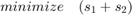
As an example they considered three wires, each consisting of 5 segments. The problem parameters are the segment widths for each wire (wij), the spacing between the three wires (s1, s2) and the inverse of the spacings between individual segments (tij). The problem can be formulated as the following in Semi Definte programing:


where  is the dominant time constant proposed by authors instead of Elmore delay,
  is the conducatance matrix and
  is the capacitance matrix that are formed in the RC equivalent circuit of the three wires example.
Wire sizing and spacing can be pictorially represented as below:
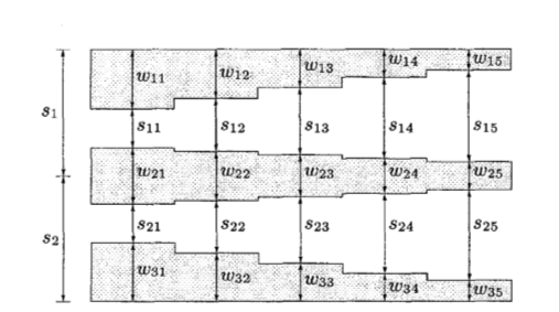
RC Equivalent of the above probem can be represented as:
Three parallel wires consisting of five segments each. The conductance and capacitance of the jth segment of wire i is proportional to  . There is a capacitive coupling between the ith segments of wires 1 and 2, and between the
  segments of wires 2 and 3, and the value of this parasitic capacitance is inversely proportional to
  , and
, and  respectively. The optimization variables are the 15 segment widths and the distances
  and
and  values.
3. Data Sources & Assumptions
The data is generated according to the same numerical example in the paper, with the following assumptions: They considered an example with three wires, each consisting of five forming in total of 15 segments widths which acts as optimization variables.
Parameters of Circuit:
n = 6;         % represents number of nodes on each wire.
N = 3*n;       % total number of nodes (18 nodes)
m = n-1;       % represents number of segments on each wire
alpha = 1;     % conductance per segment is is alpha*size
beta = 0.5;    % capacitance per segment is twice beta*size
gamma = 2;     % coupling capacitance is twice gamma*distance
G0 = 100;      % source conductance
C01 = 10;      % load of first wire
C02 = 20;      % load of second wire
C03 = 30;      % load of third wire
wmin = 0.1;    % minimum width
wmax = 2.0;    % maximum width
smin = 1.0;    % minimum distance between wires
smax = 50;     % upper bound on s1 and s2  (meant to be inactive)
All the capacitance are formulated as a matrix. CC = zeros(N*N, 5*m+3);
constant capacitance terms for the three wires are termed as:
CC(N*(n-1)+n,1) = C01;
CC(N*(2*n-1)+2*n,1) = C02;
CC(N*(3*n-1)+3*n,1) = C03;
Loop for capacitances to ground at each segment of three wires:
for i=1:m

   % first wire
   CC([(i-1)*N+i, i*N+i+1], i+1) = beta*[1;1];

   % second wire
   CC([(n+i-1)*N+n+i, (n+i)*N+n+i+1], m+i+1) = beta*[1;1];

   % third wire
   CC([(2*n+i-1)*N+2*n+i, (2*n+i)*N+2*n+i+1], 2*m+i+1) = beta*[1;1];

end;
Coupling capacitors(CC) of the circuit:
for i=1:m

   % CC between first and second wire
   CC([(i-1)*N+i, (i-1)*N+n+i, ...
       (n+i-1)*N+i, (n+i-1)*N+n+i], 3*m+1+i) ...
   = CC([(i-1)*N+i, (i-1)*N+n+i, ...
         (n+i-1)*N+i, (n+i-1)*N+n+i], 3*m+1+i) + gamma*[1;-1;-1;1];

   CC([i*N+i+1, i*N+n+i+1, (n+i)*N+i+1, (n+i)*N+n+i+1], 3*m+1+i) ...
   = CC([i*N+i+1, i*N+n+i+1, (n+i)*N+i+1, (n+i)*N+n+i+1], 3*m+1+i) ...
      + gamma*[1;-1;-1;1];

   % CC between second and third wire
   CC([(n+i-1)*N+n+i, (n+i-1)*N+2*n+i, (2*n+i-1)*N+n+i, ...
       (2*n+i-1)*N+2*n+i], 4*m+1+i) ...
   = CC([(n+i-1)*N+n+i, (n+i-1)*N+2*n+i, (2*n+i-1)*N+n+i, ...
         (2*n+i-1)*N+2*n+i], 4*m+1+i) + gamma*[1;-1;-1;1];

   CC([(n+i)*N+n+i+1, (n+i)*N+2*n+i+1, ...
       (2*n+i)*N+n+i+1, (2*n+i)*N+2*n+i+1], 4*m+1+i) ...
   = CC([(n+i)*N+n+i+1, (n+i)*N+2*n+i+1, ...
         (2*n+i)*N+n+i+1, (2*n+i)*N+2*n+i+1], 4*m+1+i) ...
     + gamma*[1;-1;-1;1];

end;
Conductance formulated as a matrix:
GG = zeros(N*N, 5*m+3);

% Constant conductance terms for the three wires are termed as:
GG(1,1) = G0;
GG(n*N+n+1,1) = G0;
GG(2*n*N+2*n+1,1) = G0;

% COnductance for each segment
for i=1:m

   % first wire
   GG([(i-1)*N+i, (i-1)*N+i+1, i*N+i, i*N+i+1], i+1) ...
   = GG([(i-1)*N+i, (i-1)*N+i+1, i*N+i, i*N+i+1], i+1) ...
     + alpha*[1;-1;-1;1];

   % second wire
   GG([(n+i-1)*N+n+i, (n+i-1)*N+n+i+1, ...
       (n+i)*N+n+i, (n+i)*N+n+i+1], m+i+1) ...
   = GG([(n+i-1)*N+n+i, (n+i-1)*N+n+i+1, ...
         (n+i)*N+n+i, (n+i)*N+n+i+1], m+i+1) + alpha*[1;-1;-1;1];

   % third wire
   GG([(2*n+i-1)*N+2*n+i, (2*n+i-1)*N+2*n+i+1, ...
       (2*n+i)*N+2*n+i, (2*n+i)*N+2*n+i+1], 2*m+i+1) ...
   = GG([(2*n+i-1)*N+2*n+i, (2*n+i-1)*N+2*n+i+1, ...
         (2*n+i)*N+2*n+i, (2*n+i)*N+2*n+i+1], 2*m+i+1) ...
     + alpha*[1;-1;-1;1];

end;
4. Solution:
Calculation of the solution for two different time delays:
delays = [130 90];
sizes = [];

for i = 1:2

    delay = delays(i);
    cvx_begin
        variables w(3*m) t(2*m) s1(1) s2(1)
        minimize(s1+s2)
        subject to
            delay*reshape(GG*[1;w;zeros(2*m+2,1)],N,N)-reshape(CC*[1;w;t;0;0],N,N) == semidefinite(N)

            w >= wmin
            w <= wmax
            t >= 0
            t <= 1/smin

            % The second and third constraints can be formulated as Linear
            % matrix inequality(LMI)

            for i = 1:m
                LMI1 = [t(i)+s1-w(i)-0.5*w(m+i) 0                       2                      ;
                        0                       t(i)+s1-w(i)-0.5*w(m+i) t(i)-s1+w(i)+0.5*w(m+i);
                        2                       t(i)-s1+w(i)+0.5*w(m+i) t(i)+s1-w(i)-0.5*w(m+i)];
                LMI1 == semidefinite(3)
                LMI2 = [t(m+i)+s2-w(2*m+i)-0.5*w(m+i) 0                             2                            ;
                        0                             t(m+i)+s2-w(2*m+i)-0.5*w(m+i) t(m+i)-s2+w(2*m+i)+0.5*w(m+i);
                        2                             t(m+i)-s2+w(2*m+i)+0.5*w(m+i) t(m+i)+s2-w(2*m+i)-0.5*w(m+i)];
                LMI2 == semidefinite(3)
            end
    cvx_end
    sizes = [sizes [w;t;s1;s2]];
end
5. Visualization of results:
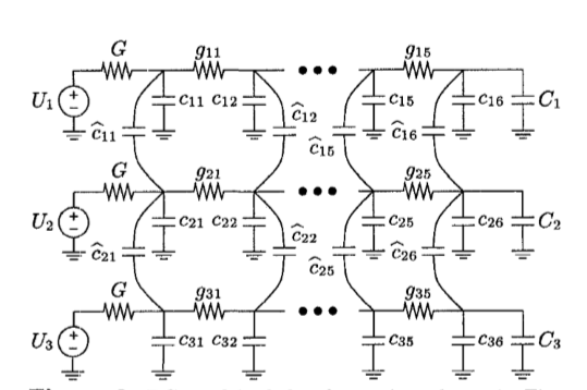
5.1 Solution1:
Solution with dominant time delay of 130:
figure(1);
hold off;
colormap(gray);

w1 = sizes(1:m,1);
w2 = sizes(m+[1:m],1);
w3 = sizes(2*m+[1:m],1);
s1 = sizes(5*m+1,1);
s2 = sizes(5*m+2,1);

x = zeros(10,1);
x([1:2:2*m-1],:) = [0:m-1]';
x([2:2:2*m],:) = [1:m]';

width1 = zeros(2*m,1);
width1([1:2:2*m-1]) = s1+s2-w1;
width1([2:2:2*m]) = s1+s2-w1;

width2a = zeros(2*m,1);
width2a([1:2:2*m-1]) = s2+w2/2;
width2a([2:2:2*m]) = s2+w2/2;
width2b = zeros(2*m,1);
width2b([1:2:2*m-1]) = s2-w2/2;
width2b([2:2:2*m]) = s2-w2/2;

width3 = zeros(2*m,1);
width3([1:2:9]) = w3;
width3([2:2:10]) = w3;

plot([x;flipud(x);0], [width1;(s1+s2)*ones(size(x));width1(1)],'-', ...
     [x;flipud(x);0], [width2a;flipud(width2b);width2a(1)], '-', ...
     [x;flipud(x);0], [width3;zeros(size(x));width3(1)], '-');
axis([-0.1, m+0.1,-0.1, s1+s2+0.1]);
hold on
fill([x;m;0]',[width1;s1+s2;s1+s2]', 0.9*ones(size([x;m;0]')));
fill([x;flipud(x)]',[width2a;flipud(width2b)]', ...
     0.9*ones(size([x;x]')));
fill([x;m;0]',[width3;0;0]', 0.9*ones(size([x;0;0]')));
caxis([-1,1])
plot([x;flipud(x);0], [width1;(s1+s2)*ones(size(x));width1(1)],'-', ...
     [x;flipud(x);0], [width2a;flipud(width2b);width2a(1)], '-', ...
     [x;flipud(x);0], [width3;zeros(size(x));width3(1)], '-');

set(gca,'XTick',[0 1 2 3 4 5 ]);
set(gca,'YTick',[0 1 2 3 4 5 6]);
title('Figure1:Solution with dominant time delay of 130sec');


%%%%%%%%%%  step responses for first solution  %%%%%%%%%%

% conductance and capacitance
G = reshape(GG*[1;sizes(:,1)],N,N);
C = reshape(CC*[1;sizes(:,1)],N,N);

% state space model
A = -inv(C)*G;
B = inv(C)*G*[ones(n,1), zeros(n,2); zeros(n,1), ones(n,1), zeros(n,1);
              zeros(n,2), ones(n,1)];
CCC = eye(N);
D = zeros(N,3);

% calculate response to step at 1st input
figure(2); hold off;

T = linspace(0,2*delays(1),1000);
[Y1,X1] = step(A,B,CCC,D,1,T);
hold off; plot(T,Y1(:,[n,2*n,3*n]),'-');  hold on;
text(T(1000),Y1(1000,n),'v1');
text(T(1000),Y1(1000,2*n),'v2');
text(T(1000),Y1(1000,3*n),'v3');
axis([0 2*delays(1) -0.1 1.1]);

% show dominant time constant
plot(delays(1)*[1;1], [-0.1;1.1], '--');

set(gca,'XTick',[0 100 200]);
set(gca,'YTick',[0 0.5 1]);
title('Figure2:The voltages at the output node due the step applied at 1st wire');


% response to step at 2nd input
figure(3);  hold off;

[Y2,X2] = step(A,B,CCC,D,2,T);
hold off; plot(T,Y2(:,[n,2*n,3*n]),'-');  hold on;
text(T(1000),Y2(1000,n),'v1');
text(T(1000),Y2(1000,2*n),'v2');
text(T(1000),Y2(1000,3*n),'v3');
axis([0 2*delays(1) -0.1 1.1]);

plot(delays(1)*[1;1], [-0.1;1.1], '--');

set(gca,'XTick',[0 100 200]);
set(gca,'YTick',[0 0.5 1]);
title('Figure3:The voltages at the output node due the step applied at 2nd wire.');


% response to step at 3rd input
figure(4);  hold off;

[Y3,X3] = step(A,B,CCC,D,3,T);
hold off; plot(T,Y3(:,[n,2*n,3*n]),'-');  hold on;
text(T(1000),Y3(1000,n),'v1');
text(T(1000),Y3(1000,2*n),'v2');
text(T(1000),Y3(1000,3*n),'v3');
axis([0 2*delays(1) -0.1 1.1]);

plot(delays(1)*[1;1], [-0.1;1.1], '--');

set(gca,'XTick',[0 100 200]);
set(gca,'YTick',[0 0.5 1]);
title('Figure4:The voltages at the output node due the step applied at 3rd wire.');

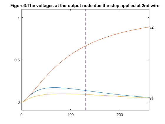
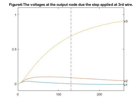
The dashed line marks the dominant time constant.
5.2 Solution2:
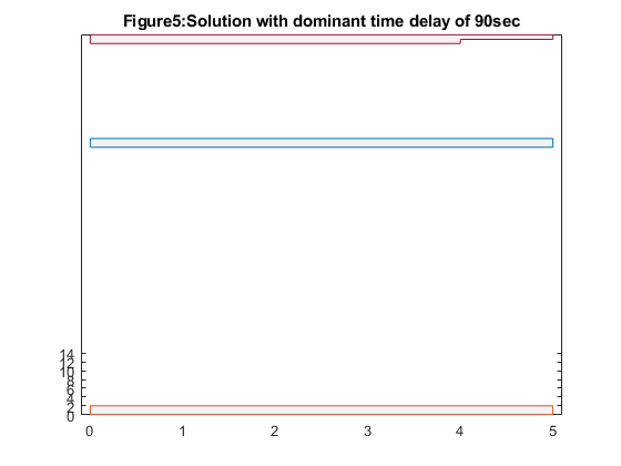
Solution with dominant time delay of 90sec
figure(5); hold off;
colormap(gray);

w1 = sizes(1:m,2);
w2 = sizes(m+[1:m],2);
w3 = sizes(2*m+[1:m],2);
s1 = sizes(5*m+1,2);
s2 = sizes(5*m+2,2);

x = zeros(10,1);
x([1:2:2*m-1],:) = [0:m-1]';
x([2:2:2*m],:) = [1:m]';

width1 = zeros(2*m,1);
width1([1:2:2*m-1]) = s1+s2-w1;
width1([2:2:2*m]) = s1+s2-w1;

width2a = zeros(2*m,1);
width2a([1:2:2*m-1]) = s2+w2/2;
width2a([2:2:2*m]) = s2+w2/2;
width2b = zeros(2*m,1);
width2b([1:2:2*m-1]) = s2-w2/2;
width2b([2:2:2*m]) = s2-w2/2;

width3 = zeros(2*m,1);
width3([1:2:9]) = w3;
width3([2:2:10]) = w3;

plot([x;flipud(x);0], [width1;(s1+s2)*ones(size(x));width1(1)],'-', ...
     [x;flipud(x);0], [width2a;flipud(width2b);width2a(1)], '-', ...
     [x;flipud(x);0], [width3;zeros(size(x));width3(1)], '-');
axis([-0.1, m+0.1,-0.1, s1+s2+0.1]);
hold on
fill([x;m;0]',[width1;s1+s2;s1+s2]', 0.9*ones(size([x;m;0]')));
fill([x;flipud(x)]',[width2a;flipud(width2b)]', ...
     0.9*ones(size([x;x]')));
fill([x;m;0]',[width3;0;0]', 0.9*ones(size([x;0;0]')));
caxis([-1,1])
plot([x;flipud(x);0], [width1;(s1+s2)*ones(size(x));width1(1)],'-', ...
     [x;flipud(x);0], [width2a;flipud(width2b);width2a(1)], '-', ...
     [x;flipud(x);0], [width3;zeros(size(x));width3(1)], '-');

set(gca,'XTick',[0 1 2 3 4 5 ]);
set(gca,'YTick',[0 2 4 6 8 10 12 14]);
title('Figure5:Solution with dominant time delay of 90sec');


% Reshaping the step responses for the dominant time constant of 90sec.

% conductance and capacitance
G = reshape(GG*[1;sizes(:,2)],N,N);
C = reshape(CC*[1;sizes(:,2)],N,N);

% state space model
A = -inv(C)*G;
B = inv(C)*G*[ones(n,1), zeros(n,2); zeros(n,1), ones(n,1), zeros(n,1);
              zeros(n,2), ones(n,1)];
CCC = eye(N);
D = zeros(N,3);


% calculate response to step at 1st input
figure(6); hold off;

T = linspace(0,2*delays(2),1000);
[Y1,X1] = step(A,B,CCC,D,1,T);
hold off; plot(T,Y1(:,[n,2*n,3*n]),'-');  hold on;
text(T(1000),Y1(1000,n),'v1');
text(T(1000),Y1(1000,2*n),'v2');
text(T(1000),Y1(1000,3*n),'v3');
axis([0 2*delays(2) -0.1 1.1]);

% show dominant time constant
plot(delays(2)*[1;1], [-0.1;1.1], '--');

set(gca,'XTick',[0 50 100 150]);
set(gca,'YTick',[0 0.5 1]);
title(' Figure6:The voltages at the output node due the step applied at 1st wire.');


% response to step at 2nd input
figure(7);  hold off;

[Y2,X2] = step(A,B,CCC,D,2,T);
hold off; plot(T,Y2(:,[n,2*n,3*n]),'-');  hold on;
text(T(1000),Y2(1000,n),'v1');
text(T(1000),Y2(1000,2*n),'v2');
text(T(1000),Y2(1000,3*n),'v3');
axis([0 2*delays(2) -0.1 1.1]);

plot(delays(2)*[1;1], [-0.1;1.1], '--');
text(delays(2),-0.1,'T');
set(gca,'XTick',[0 50 100 150]);
set(gca,'YTick',[0 0.5 1]);
title('Figure7:The voltages at the output node due the step applied at 2nd wire.');


% response to step at 3rd input
figure(8);  hold off;

[Y3,X3] = step(A,B,CCC,D,3,T);
hold off; plot(T,Y3(:,[n,2*n,3*n]),'-');  hold on;
text(T(1000),Y3(1000,n),'v1');
text(T(1000),Y3(1000,2*n),'v2');
text(T(1000),Y3(1000,3*n),'v3');
axis([0 2*delays(2) -0.1 1.1]);

plot(delays(2)*[1;1], [-0.1;1.1], '--');

set(gca,'XTick',[0 50 100 150]);
set(gca,'YTick',[0 0.5 1]);
title('Figure8:The voltages at the output node due the step applied at 3rd wire.');
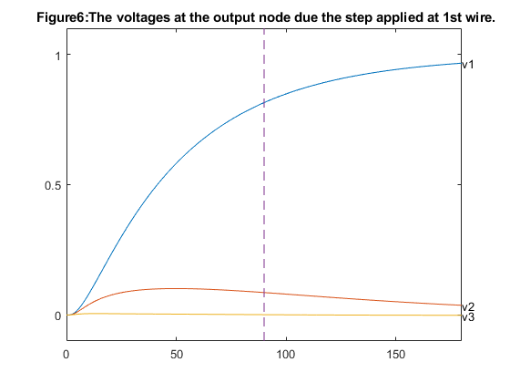
The dashed line marks the dominant time constant.
6. Analysis and conclusions:
From the observation in the first case, that is dominant time constant of 130 sec we notice that from figure1 the widest wire is number three since it drives the largest load, and the narrowest wire is number one which drives the smallest load. We also see that the smallest distance between the wires is equal to its minimum allowed value of 1.0 which means that the cross coupling did not affect the optimal spacing between the wires and from the figures 2,3 & 4 the output voltages for steps applied to one of the wires, while the two other input voltages remains zero. Where as from the second case of dominant time constant of 90sec from figure 5 we notice that the distance between the second and third wires is larger than the minimum allowed value of 1.0 and from the figures 6,7 & 8 the output voltages for steps applied to one of the wires, while the two other input voltages remains zero.
Conclusion: On comparing the two solution we observe that minimizing the dominant time constant makes the crosstalk peak shorter in time (since the dominant time constant determines how fast all voltages settle around their steady-state value). Indirectly, this also tends to make the magnitude of the peak smaller which can be seen by comparing the crosstalk levels for the two solutions in the examples.
7. Links & References:
- Lieven Vandenberghe., Stephen Boyd. & Abbas El Gama1 ,"Optimal Wire and Transistor Sizing for Circuits with Non-Tree Topology",DOI: 10.1109/ICCAD.1997.643528
- Lieven Vandenberghe., Stephen Boyd. & Abbas El Gama1,"Optimizing Dominant Time Constant in RC Circuits", Link:http://www.seas.ucla.edu/~vandenbe/publications/rc_final.pdf
- This was made successful with the help of CVX toolbox which allowed us to solve the problem and reproduce the results sucessfully.