
My research focuses on micro-nanofabrication process technology, though we also work on various device applications. We use the facilities at the three cleanrooms in campus: G2N, Quantum nanoFAB and CIRFE. We are also a very heavy user of Watlab, particularly its SEM/EBL and FIB system.
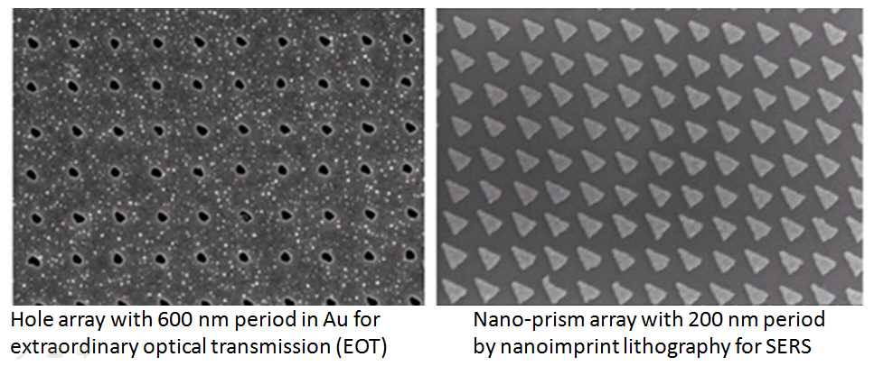
The fastest way to gain a feeling of my research is by going through my presentation given as invited talk at universities and conferences. Here are some typical nanostructures we fabricated.
Overview
Nanoscale science and technology is one of the fastest growing research areas in recent years. Nanofabrication techniques are the cornerstone for this rapid growth; without this capability, nanotechnology would be a mere speculation. In fact, while the birth of nano-science/technology was occurred over fifty years ago, from Richard Feynman’s famous 1959 lecture “There's Plenty of Room at the Bottom”, growth in this field was rather slow in its first 30 years - mainly due to the lack of nanofabrication capability. It is only since the mid-1990s that nano-research has experienced explosive grown, coinciding with the development and more availability of a broad range of nanofabrication techniques.
There are two approaches to enabling fabrication at the nanoscale: “bottom-up”, which involves chemical synthesis and self-assembly, and “top down”, where nanostructures are generated or duplicated by lithography. For the “top-down” method, electron beam lithography (EBL), focused ion beam (FIB) etching/lithography and nanoimprint lithography (NIL) are generally used to create or duplicate nano-structures.I. 1 Nanofabrication - Electron beam lithography
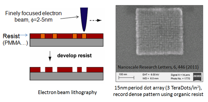
Electron beam lithography (EBL) is the most popular nano-lithography method for R&D, device prototyping and photo-mask manufacturing. It uses an focused electron beam to expose the resist, to make it more soluble (positive tone) or less soluble (negative tone) in the developer. It has demonstrated sub-5 nm resolution.
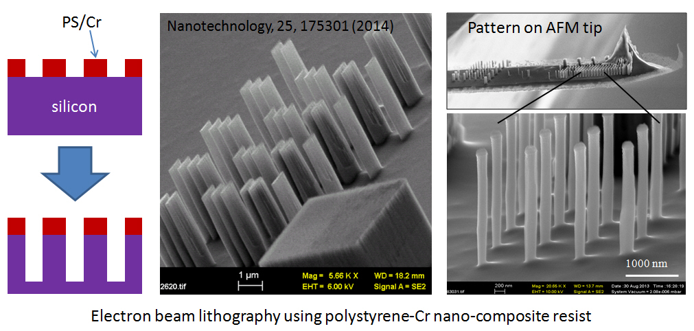
We systematically studied negative resist polystyrene, and achieved both ultra-high resolution (15 nm pitch) when using low molecular weight, and ultra-high sensitivity (1 µC/cm2) when using high molecular weight. We have also shown that low cost broad disperse polystyrene performs as well as the high cost narrow disperse polystyrene. Moreoever, demostreated that polystyrene can be evaporated, which, unlike spin-coating, can be applied to any irregular surface such as an AFM tip or optical fiber. Lastly, by adding Cr to the evaporated polystyrene resist, the etching selectivity to silicon is greatly incrased, making it possible to etch very high aspect ratio silicon structures using the polystyrene-Cr nanocomposite resist.
I. 2 Nanofabrication - nanoimprint lithography
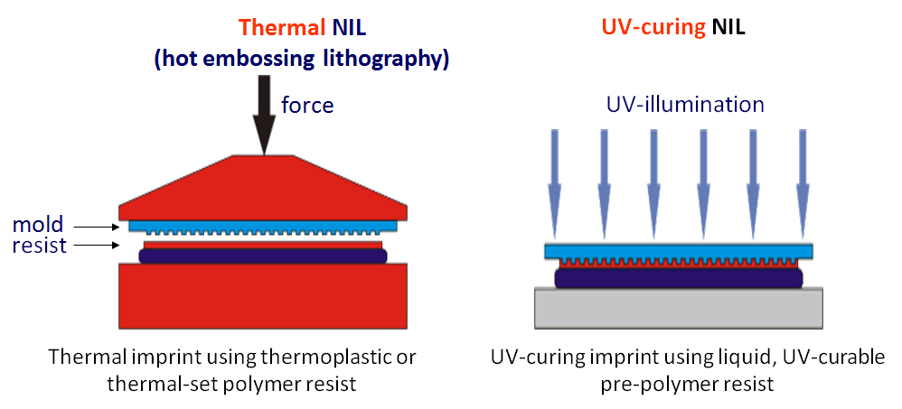
Nanoimprint lithography (NIL) relies on the mechanical conformation of a low viscosity resist to the structures of a mold. It offers high resolution (2 nm), high throughput (up to one wafer/minute), low cost and high pattern transfer fidelity. Except for semiconductor industry where advanced photolithography will continue to be the workhorse for the coming years, NIL is considered as the most promising nanolithography for mass production of nanostructured devices simply because other nanolithographies (e-beam lithography, focused ion beam, scanning probe lithography…) are too slow and costly for volume production.
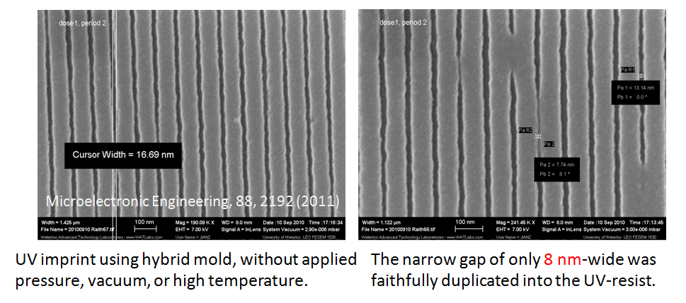
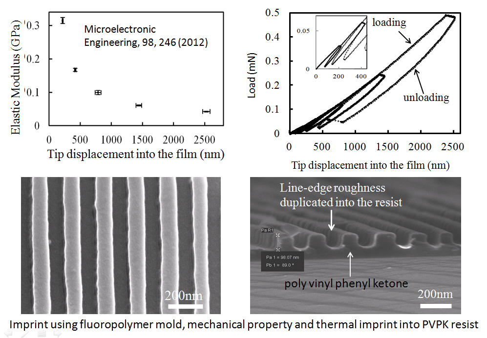
We demonstrated hybrid nanoimprint soft lithography with a resolution down to 8 nm, without the use of applied pressure, elevated temperature (resist cured by UV irradiation at room temperature), or vacuum. This process uses a mold consisting of a hard top layer on a soft PDMS (polydimethylsiloxane) sheet that is able to form intimate contact to the UV-curing resist. In addition, as it is often costly to fabricate the mold for nanoimprint lithogrpahy, we developed a process that first duplicates the pattern on a master silicon mold (costly to fabricate, britten thus easy to break) into a fluorpolymer that has low surface energy for easy demolding, then use the duplicated mold to imprint into the resist. As such, the expensive master mold is saved.
II. Nanostructured Plasmonic Bio- and Chemical Sensors
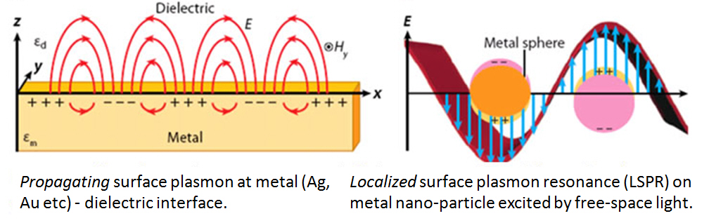
Surface plasmon is an evanescent surface electromagnetic wave caused by collective and coherent free electron oscillation at a metal-dielectric interface. SPR (surface plasmon resonance, including propagating SPR when the metal film is continuous and localized SPR for isolated metal nanostructures) refers the excitation of surface plasmon by light. As the surface plasmon is confined to the metal-dielectric interface with an extension of only ~200nm from the interface, its resonant frequency is highly sensitive to the refractive index change at the interface. For example, binding of a monolayer of (bio-) molecules on the metal surface will lead to a detectable shift of resonant wavelength; therefore, SPR can be used as bio-sensor with high sensitivity to detect in real time biological binding events, such as DNA hybridization and antigen-antibody binding.
III. Additional Research
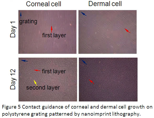
Additional research thrusts include electrochemical biosensors consisting of nano-electrode arrays for improved sensitivity, contact guidance of cell growth for tissue repair, guided growth of carbon nanotubes, fabrication of contrast agent for medical ultrasonic imaging…
In short, my group is open to any research topics where nanofabrication plays a critical role.

University of Waterloo
200 University Avenue West
Waterloo, Ontario, Canada N2L 3G1
Email: bcui@uwaterloo.ca
519 888 4567 ext 38754
contact us | give us feedback | Electrical and Computer Engineering